Hardware:
The clock circuit presented last time had problems. The two new clocks were non overlapping but due to the delay introduced would try demodulating the wrong channel. I tried re-working the circuit by delaying the LED driving clocks. In the end, this approach was just too complicated and I abandoned it.
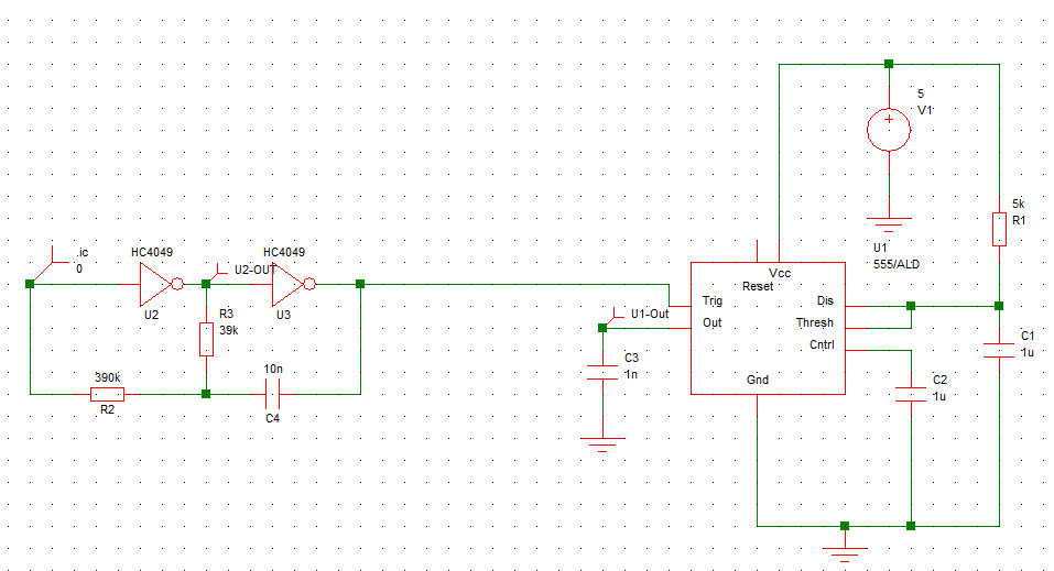
As a replacement I adopted a circuit designed by Shanit. A relaxation oscillator was combined with a 555-timer in monostable operation to one shot a variable duty cycle. This output was then passed through an inverter. The result is a de-modulation clock with reduced duty cycle from the original CLK but not overlapping onto secondary channel.
What I learned: If something is starting to appear too complicated, ditch it and adopt the simpler topology.
Below is a schematic of the circuit I ended up using. The datasheet recommended I use a 1 uF with 5k POT to create a variable duty cycle. I built the circuit on the breadboard and have been using that to test the overall system. On Monday, Jon will construct an actual board which can be mounted on the POX board. Another great idea adopted by Shanit was to cut the Enable lines (EN1, EN2) and use them for the S/H demodulator clock line. In this way, the board won't look like such a hacked together nightmare.
There are a couple last minute changes Jon and I will be making to the board next week. We'll be fine tuning the gain of the TIA section and maybe making fine tuning changes to the LP filter.
Software:
Some tremendous progress was made on the software solution. In the last post I had discussed the DC detection, automatic detection and PGA gain. I've seen some other interesting solutions and am confident in my result. For instance, team Tango has a step-up PGA gain going from (1,2,5,10,20, etc.) till it reaches max rail. If I could return, I would most likely implement this solution. I like the elegance and the fact that it requires almost no error checking code.
My efforts last week:
1. Implement detection, subtraction, and PGA on both channels. Complete
2. Implement TCP/IP send back for both channels. Complete
To test this I drove a simulated PPG signal into the DC subtracter circuit and let my program run. It was actually very easy (think Copy/Paste) to implement the Ch2 code. I have a parallel system now where all actions are taken side by side in steps.
My focus this weekend and the next week is as follows:
1. Implement a peak detection scheme to calculate heart rate (in bpm).
2. Use peak detection scheme with a newly created SpO2 .VI detector to output the saturated blood oxygen level.
3. Fine tune the software to make it more/less aggressive. Right now, the output from the TIA is about 50 mV p2p so the gain is really trying to do gain 100 or 200. There are times when the output saturates which means I need to write error detection.
4. Error detection code.
I've created a thorough simulation of both of these components in LabVIEW and will update tmmrw or Sunday with a showing of the program. Basically, I wanted a test bench to test this code on my computer before I push changes to a micro controller.
I'm trying to figure out if any of these simulations or code would be helpful in an open source repository. I'd like to provide some thorough documentation and upload them as a project to Sourceforge or the LabVIEW example database (I wanted to check licensing agreement).
If anyone reads this blog and wants to contact me, my email is nlshrake@ucdavis.edu.
No comments:
Post a Comment