Monday, April 26, 2010

Progress Report Update

We made some good progress in todays Lab meeting. Our efforts are now focused on development of the software for interfacing with Channel 1,2 and populating the rest of the board.

Today, Jon populated channel 2 on our two development boards. We replicated the original component values that were specified in the initial channel 1 design. We hope by making this choice that software design will be simplified as hardware will be uniform.

Today, I continued my effort to implement my Digital IIR Filter on the micro controller. In my last post I documented the development cycle of a simulation I ran. The actual process of implementing the subvi on the micro-controller was difficult.

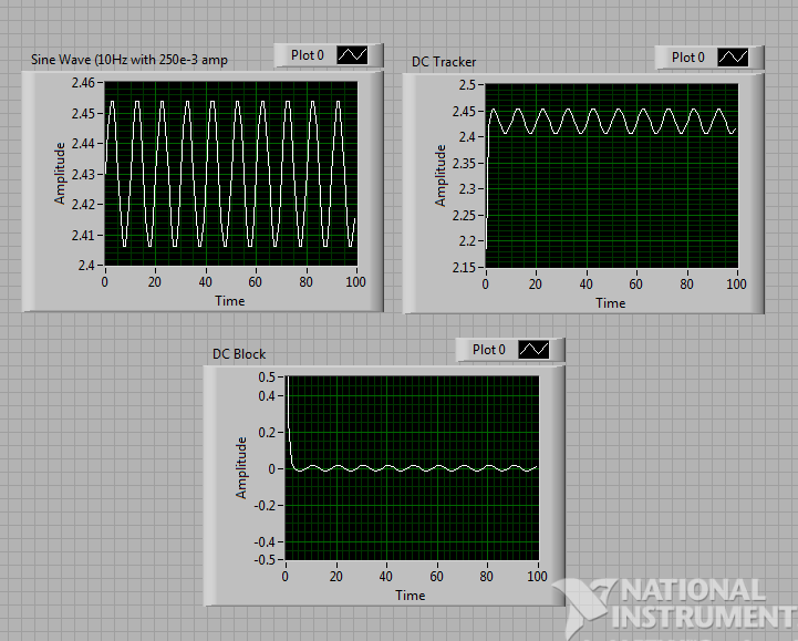
The problem I ran into was trying to verify that the ADC values were in fact being sent to an array. It's critical that the values be stored in some dataset because the digital filter operates on past values. I discovered that the JTAG interface does not send array contents back so the VI front panel was not updating. A quick hack suggested by Cevin was to use the OLED to display array contents. I had the screen output the i-1 item in the array so that it was always displaying the previous updated array item. In this way, I was able to verify that the data was being stored. After concluding that the data was stored I proceeded to implement the DC Filter as a subvi. Everything worked out of the box and the program now shows a DC offset from output of ADC.

In the future, I'd like to link the ADC array output back to the computer so I can debug more thoroughly and plot the ADC output.

Goals for next week:
1. Fully operational TIA section. I will be going back and increasing the feedback resistor to bring the signal closer to 5 volts. I'll likely need to performing a stability analysis and perform some form of compensation to decrease the oscillation. I will provide an update later this week on my efforts.

2. Improve performance of POX Software Controller. Right now I've split many of the components into SubVI's. Now that the program can determine DC bias I will be creating a software solution to modify DC bias dynamically from this input. For instance, today in lab I observed that the output from the DC Tracker was 2240 corresponding to analog voltage of around 2.69v. In the future I want to be able to push this DC offset to 2.5v so I will have to dynamically modify the DAC value for DC subtraction.

I will also this week be integrating this with the ability to increase gain in the PGA stage. I had implemented the PGA as a SubVI but this isn't working. I think labview doesn't like elemental IO pins in subvi so I need to figure that out. So goal this week is to be able to give a PGA gain of 200 and keep DC offset at steady 2.5v auto.

3. Jon is work on testing the channel 2 and fixing all problems.

4. Megan is running a simulation in LabVIEW. The simulation will entail a mock gain session on a sinusoid with a random AC amplitude. The program will be adaptive and try to take full scale of the ADC. Therefore, the program will required some conditional logic to determine if PGA is possible if it won't saturate. The program will also have ability to add smaller AC bias from increasing brightness of LED.

This is really just a simulation but the reasoning will serve how we make our adaptive process to modify parameters to get full scale performance from ADC.

Saturday, April 24, 2010

DC Block Digital Filter Simulations

Progress was made in regard to implementation of the DC Blocker and detector. As explained previously, we want to take full advantage of the ADC so we use a PGA to provide a variable gain. The PGA operates on a reference DC bias of 2.5v and provides gain to any AC on this DC line. However, the signal that arrives from TIA and after S/H circuit has some random nonzero DC bias associated. This DC bias needs to be detected and removed to analyze just the AC component.

While an analog filter could be used to remove the DC, an analog circuit would have to be developed to detect DC bias. A better solution is to implement a digital filter on chip. This was accomplished with minimal experience with DSP. An IIR filter was simulated first in MATLAB to quickly analyze and confirm results. Then the solution was transfered to a LABVIEW environment as will eventually be encapsulated as a Sub-VI for integration in full software.

DC removal transfer function:
DC Tracking transfer function:

To simulate with MATLAB the transfer function was implemented in the 1D filter function. A link is provided below.

Figure1,2: Random 1 volt bias applied with DC tracking no noise. Random 2.3 volt bias applied with some noise.
http://www.mathworks.com/access/helpdesk/help/techdoc/ref/filter.html

Next, I worked to implement this in the LABVIEW environment. I ran into early problems with lack of documentation. I desired a solution as simple as MATLAB's 1D filter function that allowed me to simply specify filter transfer function coefficients. Most IIR filter examples I found for LABVIEW were about using Elliptical, Butterworth, etc. filters. I did finally find a control 'IIRFilter' that allowed me to specify forward and reverse coefficients. The result is presented below.


I wanted to leave some space to discuss issue of precision. MATLAB and LABVIEW allow for 64-bit double precision. But on a DSP chip the precision might be much lower. Our design was simple enough with a low precision coefficient (alpha=0.9). I will comment in more detail on this in a later post.

Sunday, April 18, 2010

Further Discussion on Software

As Nick discussed in his previous blog, we have been working on being able to operate all 4 DACs in such a manner that we can dim the LEDs as necessary using DACs 3 & 4, and be able to subtract out DC values using DACs 1 & 2. As of now, we have a program that allows us to run through the DACs, changing input values as necessary. In the near future, this program will need to be implemented in a manner where there is no longer a user defined interface, although that the computer will be programmed in such a way that it is making all of the necessary adjustments to our heart monitor signal through input coming from the ADC.

Problem statement #1: The ADC will take in an input signal, which will be analyzed. In the computer analysis, the signal will have an AC signal riding on a DC value. This exact DC value must be subtracted out, so that the signal sits on 0 V DC. This is important so that later in the system, the signal can be biased to 2.5 V allowing for the signal to swing in a dynamic range of 0-5 V. Build a program that allows the computer to calculate this DC value and is able to increment or decrement the DC value in order to have the signal sitting at 0 V DC.

Problem statement #2: As mentioned above, this signal will eventually be biased at 2.5 V. The signal then needs to use the PGA, or programmable gain amplifier to adjust it automatically to swing from 0-5 V, without having saturation.

Problem statement #3: Included above is our thoughts in having need for operating all 4 DACs and eventually operating them solely with the computer and no user input interface. This is another challenge to overcome.

Team Sierra is making progress in software situation, and most importantly identifying what the problems to overcome are. Before implementing ideas, it is important to explore the potential problems and come up with solutions to those problems. For example, it may be easy enough to identify a DC value from knowing the maximum and minimum values from peak to peak of our signal range. We would need to take a sample that would be inserted in an array to allow us to do this. However, we would also have to take into account where the minimum DC value starts from. We may find the DC value from peak to peak to be 1.5 V, although the minimum value may be sitting at 0.5 V to begin with. We must be careful for troublesome points such as this. In dealing with the gain, we must decide whether the computer program will be allowed to saturate before it decides that it needs to go back one gain setting. We must make careful adjustments to the PGA. All different scenarios must be considered.

LABVIEW control

Megan and I have been working on the ability to control devices on the POX board. In the near future, a software solution will be developed to adaptively control all devices. This first bit of test code is meant to demonstrate abilities and help test and debug.

The program below offers control of all 4 DAC's. DAC 1/2 represent Channel 1/2 and offer ability to specify DC value to subtract. DAC 3/4 offer ability to control brightness of LED by adjusting bias voltage on base of transistor.

In the next work we will be integrating this control with the ADC and PGA. The adaptive software will act as a feedback system. The goal is to get maximum performance of ADC. This requires true DC subtraction and for the PPG signal to operate rail to rail (0 to +5v). To accomplish this we will have three (2) routes.

(1) modify PGA gain. This will allow major gain but steps (1, 2, 5, 10, 50, etc.) limit the maximum gain as we can't saturate.
(2) modify the brightness of LED. This will allow minor variations.


Saturday, April 17, 2010

Trans impedance progress

Today I populated the trans impedance stages. I knew from earlier experiment that a photo diode of similar specifications provided a 88 uA current for an enclosed setup. This enclosed setup mimicked the shielding provided by the probe. I also had to fix the V(+) and V(-) error by cutting traces and rerouting. I followed the guide that was posted under TIAfix.pdf.


The two stage differential trans impedance amplifier above allows for current to voltage conversion with elimination of common mode noise. While both stages can provide gain, I choose to provide gain in stage 1 and have stage 2 as a differential follower. I wanted to bring the output voltage to about 500 mV. I selected a 20k resistor in the feedback path to provide an estimated output voltage of 1.7 volt. The second stage will act as a differential follower such that the following is observed. I chose R1 = Rf = R2 = Rg = 50k.

R_1 = R_\mathrm{f}\,
R_2 = R_\mathrm{g}\,

 V_\mathrm{out} =  V_2 - V_1 \,\!

To test the operation of the trans impedance stage I performed the following. I drove the CLK1,2 lines on the POX board with +5v square waves from two function generators. I then use micro controller to program DAC3/4. This allowed modification of brightness of LED in probe. I then turned on the probe and observed the output from S1out, S2out, and AmpOut. As I was driving with a square wave I expected to see the same waveform (freq) on scope. I found the amplitude was below my expectations and actually was around 750mV.

The capacitors CTI1, CIT2 are implemented for stability concerns. The challenge is to prevent oscillation from occurring causing overshoot and ringing. I am preparing notes on this with details to our implementation. I will also include in these notes details on elimination of common noise and why differential amplifier is preferred selection.


I'm starting to look into software and have found some good links on DC removal for DC subtraction. Today I played with implementation in MATLAB. A 1D IIR filter can be implemented easily in MATLAB. Once we have good result in this respect we can transition development to LABVIEW environment.

Thursday, April 15, 2010

EEC136 LED Driver and Trans impedance update

The LED driver circuit was simulated and populated this week. An early problem encountered by Jon and I was that with no LED's as a load the circuit demonstrated erratic behavior. Without the probe plug, the supply produced by the regulator dropped below +5v. The DAC's also failed to provide full supply. The LED driver will produce current depending on the bias selected from the DAC3/4 from micro controller. If the current has no where to go but through the bottom transistor. This problem was remedied with construction and introduction of the finger probe.

The LED driver was tested by using the I2C DAC LABVIEW program to modify the voltage on the base of the bias transistor. The brightness was modified by changing the voltage from the peak (+5v) to (0v) transistor off. We need to investigate just how hard we can push these LED's as the brightness can improve the signal coming out of PD. To do this, we will need to modify the emitter resistance and see just how far we can push.

The finger probe was constructed in the following manner. First, a pre-prepared probe from Masimo was acquired and modified. The wire was cut and the wires were stripped. The color code is as follows:

ORANGE - LED IR
RED - RED LED
WHITE - PHOTO DIODE 1
GREEN - PHOTO DIODE 2

METAL - GND

I took a copper prototype board and cut traces. Then I soldered the wires into specific traces. I think soldered a 16-pin male connected on the POX board where the LED output and PD input's come in. Then, I soldered a 16-pin female connected to this copper prototype board. The final result is displayed below:


I'm nearing completion on the work of the transimpedance stage as well. I've populated the entire subcircuit but am running a couple of last minute simulations to choose feedback and input resistances. A problem was discovered by Shanit in which VCC and VSS are wired backwards. To remedy this, I will have to cut a trace and use jumper wires to each of the 3-vcc/vss pads. I will post another update with progress on this front in the next few days.

Megan has been given the task to complete an integrated software solution. The software solution will enable control of all 4 (four) DAC's, the PGA, and the ADC. This will allow modification of the intensity of the LED's, DC subtraction, and programming the gain amplifier. At this point the team will regroup and focus for the rest of the quarter on software development.

Wednesday, April 14, 2010

Class Discussion: Clock Timing

A clock signal must be implemented on board to drive the LED driver circuit. By repeatedly flashing LED's on an off modulation is achieved. The photons from LED's after passing through fingertip are received on a photo diode. This signal then must be demodulated back to baseband.

The question is: If the clock for S/H demodulator is out of phase or delayed from clock driving LED's then will error occur and how can it be fixed. The problem could arise from delays in the circuit. The oscillator is designed as a simple charging RC circuit with dual inverters. There exists a delay in switching of inverters.

To match clocks a phase delay of some sort must be introduced in the circuit. A simple RC delay can be introduced providing a phase of 45 degrees and can be cascaded to the desired result. This result assumes the delay is constant and a multiple of 45 degrees. A more complex delay network could be developed to provide variable tuning delay with a potentiometer or variable capacitor. If inductors are allowed in the design, then a maximum phase of 90 degrees could be achieved.

Monday, April 12, 2010

LED Driver

I (Jon) have been working on the LED driver circuit. I need to measure how much current is being fed to the LEDs to verify that the circuit is behaving as specified in my design. I am making good progress, and the LED driver circuit section of the board is populated.

Monday, April 5, 2010

Photo diode and Transimpedance update


I began construction on a circuit to experiment with photodiode and LED. First, a circuit was constructed to flash an LED. Another circuit was constructed with a photodiode to measure response to LED. Below is an idea of what the experiment looked like. Also attached are photos of the two circuits together.


The function generator was used to drive the LED’s at a specified frequency. The top of the LED was placed above the photodiode and mounted. In this manner, the output the response of the photodiode could be analyzed and quantized.

First, DC measurements were made on the constructed circuit. The diode had an open circuit voltage of around 650 mV. When the circuit was constructed with the 300k resistor though, the voltage across the diode dropped to around 280 mV. This suggests a current of a current of 88 uA. Next, the output of the photodiode was connected to the oscilloscope. I drove the LED with a square wave and observed the waveform at the photodiode output.

One thing I noticed was that an ambient light condition, a large DC bias exists. If the box was isolated and put in the dark box, then the Bias was removed. Additionally, the signal became much less noisy and clearly resembled the driving signal. Another thing I noticed was how the modulation scheme developed. The output LED’s are 180 out of phase and are switched. The switching procedure acts as a modulator shifting cardiac signal from baseband to the carrier band. In this manner, our previous circuit with high pass filter followed by Sample and Hold implements the demodulation application.

I also started looking into the topology selection for transimpedance stage. The reason for a differential stage is to eliminate common mode (CM) noise. I will update with some more information in a later blog. Below is some information on differential opamp stage extracted from Wikipedia. The key idea with this circuit is to amplify the difference between the terminals of diode.


In my next experiments, I will be implementing the transimpedance stage and analyze the approach to remove common mode noise. Additionally, I want to perform some quantization on how hard we can drive the LED’s. As we are driving the LED’s with PWM approach we can increase current through device.

Photodiode/Transimpedance Links

1. Photodiode Technical Information

http://sales.hamamatsu.com/assets/applications/SSD/photodiode_technical_information.pdf

2. Photodiode Characteristics

http://www.optics.arizona.edu/Palmer/OPTI400/SuppDocs/pd_char.pdf

3. Designing of Photodiode Amplifier circuits with OPA128

http://focus.ti.com/lit/an/sboa061/sboa061.pdf

4. OPA350 Datasheet

http://users.ece.utexas.edu/~valvano/Datasheets/OPA4350.pdf

5. Differential Operational Amplifier explanation

http://www.ecircuitcenter.com/Circuits/opdif/opdif.htm

6. Differential Operational Amplifier Stage

http://en.wikipedia.org/wiki/Operational_amplifier_applications